


Research
Back
Quantum photonic and optoelectronic devices based on nanomaterials
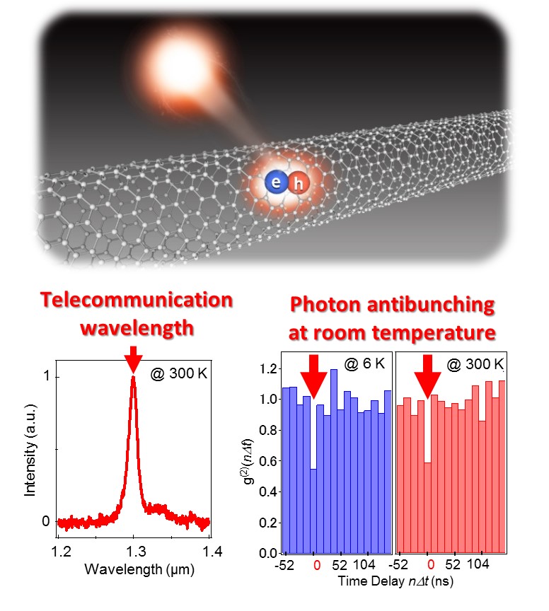
CNT-based single photon sources at telecommunication wavelength and room temperature
Photon antibunching from low dimensional materials have attracted much attention for use as single photon sources in quantum information technology such as quantum cryptography. Especially, for commercially available long-distance quantum cryptography with optical fiber, single photon sources, which can work at room temperature and telecommunication wavelength, are required. However, single photon sources at room temperature and telecommunication wavelength have not been realized by using semiconductor quantum dots. In our study, we demonstrated the first photon antibunching at telecommunication wavelength and room temperature by using carbon nanotubes. Our results revealed that the carbon nanotubes can exhibit photon antibunching over the full temperature range from 6 K to 300 K.
Publications
- “Photon antibunching in single-walled carbon nanotubes at telecommunication wavelengths and room temperature”
Takumi Endo, Junko Ishi-Hayase, and Hideyuki Maki, Appl. Phys. Lett. 106 (2015) 113106.
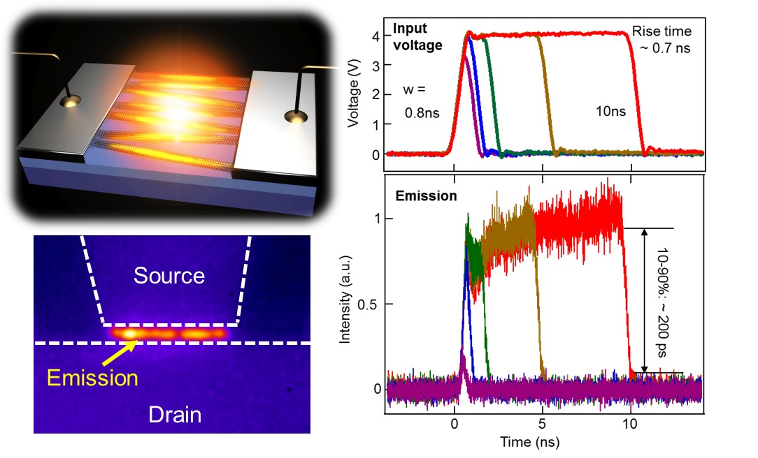
Ultrahigh-speed nanocarbon blackbody emitters integrated on silicon chips
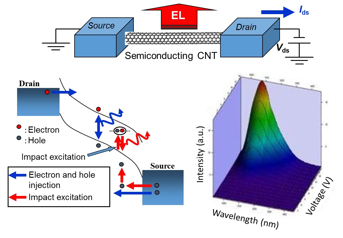
CNT-based electroluminescence (EL) emitters
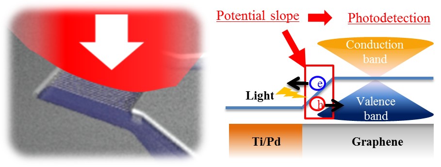
Nanocarbon photodetectors
Light emitters and photodetectors based on compound semiconductors are widely used in the areas of optical communications, sensing, spectroscopy, etc. However, these optoelectronic devices face challenges with respect to their integration with silicon-based platform because of their large footprints and low crystallinity of the compound semiconductors grown on Si wafers. On the other hand, nanocarbon materials, such as CNTs and graphene, are attractive materials for optical and optoelectronic applications. Electrically driven carbon-based emitters, which can be based on electron-hole recombination (EL emission) or blackbody radiation, and photodetectors have several advantages: a small footprint emitter can easily be obtained due to its simple fabrication process on Si wafer. These advantages could open new routes to photonics and optoelectronics integrated with silicon-based optoelectronics. We demonstrated the electrically driven, ultra-high-speed light emitter (~ GHz) and photodetectors based on nanocarbon materials on silicon chips.
Publications
- “An Electrically Driven, Ultrahigh-Speed, on-Chip Light Emitter Based on Carbon Nanotubes”
Tatsuya Mori, Yohei Yamauchi, Satoshi Honda, Hideyuki Maki, Nano Letters, 14, (2014) 3277.
- “Electrically driven, narrow-linewidth blackbody emission from carbon nanotube microcavity devices”
M. Fujiwara, D. Tsuya, and H. Maki, Appl. Phys. Lett., 103 (2013) 143122.
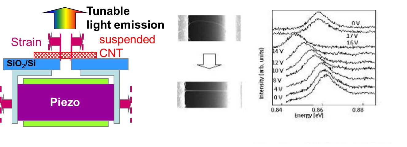
Tunable bandgap engineering for nanocarbon materials
Single-walled carbon nanotubes (SWNTs) are attractive material for the building block of electronic and optical nanodevices. Emission energy obtained from PL and EL is determined by the band gap that depends on the chirality of SWNT. The band gap can be tuned by the strain of SWNT and its change of the band gap depends on their chirality and deformation mode. We have fabricated the new devices for applying strain to the individual suspended SWNTs. Using this device, the processes of the deformation under stretching have been directly observed by a scanning electron microscope. From the PL measurement for the individual SWNT, the emission energy shift due to the band gap change caused by the elastic strain is observed.
Publications
- "Direct observation of the deformation and the band gap change from an individual single-walled carbon nanotube under uniaxial strain"
Hideyuki Maki, Tetsuya Sato and Koji Ishibashi, Nano Letters, 7 (2007) 890-895.
Back